
TI - Technical Info
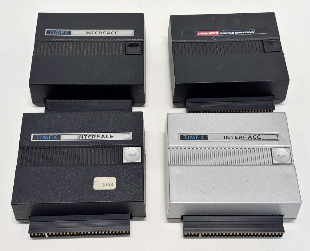
TMX Portugal has done two versions of the FDD interface: one for TC2048 (can be used with TC2068 with emulator cartridge) and one for TC2068 (this version, the reset button is silver. The rest is equal). This is because FDD interface ROM initialization works with the computer ROM. If the right version of the FDD interface isn’t used with the computer it was designed for, the computer simply crashes.
The FDD Interface
Author of this text: Jarek Adamski
FDD 3000 communicates through the FDD interface. The interface has one connection for Edge Connector and on the other side, has the connector to FDD. So you can use any type of FDD interface for any type of FDD 3000. For ZX’s who have 128 FDD interface requires special Eprom reprogramming (port conflict). Only FDD interfaces from STAVI are free of that bug.
FDD 3000 is connected to the FDD interface through spiral cable, the transfer is half duplex 6 bit ( 1 bit is STROBE, all bits can be used normally) which gives a low transfer rate.
The FDD interface is not a complex unit. Port accesible by out/in #EF.
Inside FDD is it port #0F, and MIRRORED: #2F, #4F, #6F, #8F, #AF, #CF, #EF.
Ports are connected this way: (TI BIT n MEAN BIT in Timex Interface #ef)
BIT READ WRITE NOTE
7 DREQ FDC 1772 ?
6 TI BIT 6 TI BIT 6
5 DREQ FDC 1772 ?
4 TI BIT 4 OR 7 TI BIT 4 OR 7 DEPENDS ON TI VERSION… STANDARD IS 4
3 TI BIT 3 TI BIT 3
2 TI BIT 2 TI BIT 2
1 TI BIT 1 TI BIT 1
0 TI BIT 0 TI BIT 0
The interface has also a RESET switch, and an amplifier of the CV signal, which is more accessible than at TIMEX FDD 3000 at MONITOR output (chinch). It has a lot of interferences (TTL signals in spiral cable, no shield, 1 meter long.)
But What is inside?
INSIDE FDD – PORTS, and SHORT this PORT INSIDE CHIP STERRED WHAT IT DO?
- #10 WD2123 configuration (write) CHA
- #11 WD2123 configuration (write) CHB
- #40 WD2123 data CHB
- #41 WD2123 status/command CHB
- #80 WD2123 data CHA
- #81 WD2123 status/command CHA
- #C0 FDC1770 steering port/status
- #C1 FDC1770 track port
- #C2 FDC1770 sector port
- #C3 FDC1770 data port
- #E0 HELPING helping port(below)
How to use these ports? I still wait for the info… but : PORT #E0
BIT WRITE 1 0
7 HEAD DOWN UP
6 #0000-#1FFF ROM RAM
5 DENSITY FM MFM
4 SIDE 1 0
3 DRIVE 3 ON OFF
2 DRIVE 2 ON OFF
1 DRIVE 1 ON OFF
0 DRIVE 0 ON OFF
Interface structure.
The interface looks like this:
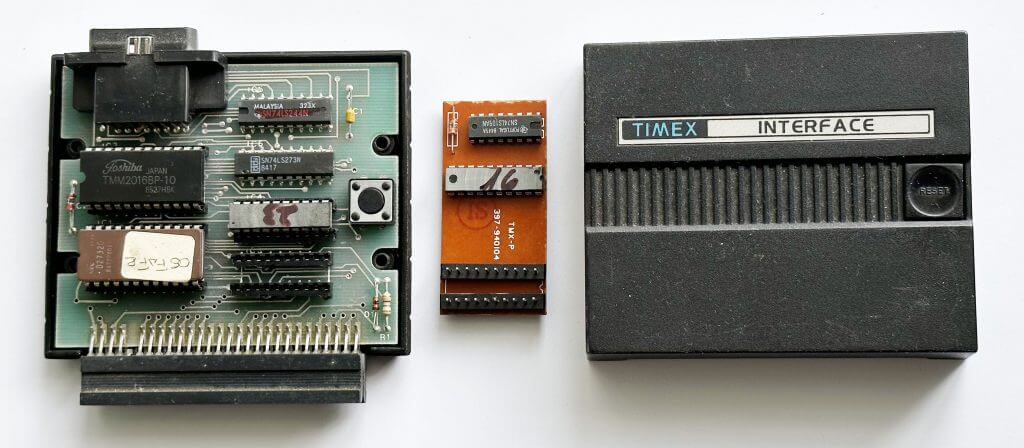
On the top is a connector to the real FDD 3000/3 below you have RAM, below EPROM, and from the top right: two line buffers. and 2 GAL’s (dolny/gorny). On the bottom, you have an edge connector.
The description of TIMEX INTERFACE, which is used to connect the computer with a ZX SPECTRUM compatible edge connector to the TIMEX FDD 3000 or Unipolbrit clones.
Interface decodes addresses:
memory : #0000 and #0008 with _M1 active – disconnection of ZX ROM.
memory : #0604 with _M1 – reconnection of ZX ROM
port #xxEF – input/output 8 bit.
After disconnection of ZX ROM interface connect his memory in the areas :
#0000..#1FFF TI (Timex Interface) ROM (4KB, two times)
#2000..#3FFF TI RAM (1KB eight times or 2KB four times)
(1) TI (Timex Interface) with double-sided PCB painted at the bottom on the green, without any numbers, at the bottom (lower side) at the center of the “SER” sign.
Components : (IC1)TMM2016 (RAM), (IC2)D2732D (ROM), (IC5)SN74LS273N (output line driver), (IC6)HD74LS244P (input line driver), (C1)473/50V, (C2)ASE4832ZIB, (D1)1N4148R, (R1)680ohm 5%, microswitch black, edge connector ZX, and DA15M connector.
Rewired connections under PAL components.
In the DA15M pins 7 and 8 are not connected. Mask of the connector: %11001111, Bits 4 and 5 not connected to 244 and 273 – in the reading state is not known. (recommended – connecting them to the unused 244 outputs, and the corresponding 244 inputs – to the ground)
(2) TI with double-sided glass laminate, yellow color, without numbers, and the visible manufacturer signs, the side holes are circular.
Elements: TMM2016, D2732D, SN74LS273N, SN74LS244N, (2x)+2.2/+25V(C), 22uF/25V, DA9C38(T), microswitch white, edge connector ZX to the soldiering, DA15M.
Unused inputs 244 and 273 are connected to the ground thru wires.
In the DA15M pins 7 and 8 are not connected and cutted. Mask of the connector: %11001111.
Bits 4 and 5 are connected thru wires to 244 – low state when read.
GAL (PAL, PALCE) chips 16V8 are connected so:
__ __ __ __
-\ CLK Io \/ | +5V A12 Io \/ | +5V /-
| A14 I I /L3 /IORQ I O /IN |F
Z| A13 I O CLK /RD I I A0 |D
X| A10 I I A15 A8 I I /WR |D
| A9 I IC3 O /ROM A11 I IC4 | nc (A1) |
B| A3 I O /RAM A7 I O /L3 |3
u| A2 I I /L2 A6 I O /L2 |0
s| /MREQ I O /L1 A5 I I /L1 |0
| /M1 I O ZXDIS A4 I O /OUT |0
-/ GND |______I GND GND |______I A1 \-
CPU inputs : A0..A15, /IORQ, /M1, /MREQ, /RD, /WR
Power : GND, +5V
TI sterring : /IN – read from port #EF (74244, pin 1 & 19)
/OUT – write to port #EF (74273, pin 11)
/RAM – activate TI RAM (2016, pin 18 & 20)
/ROM – activate TI ROM (2732D, pin 18 & 20)
ZX sterring : ZXDIS – thru 680om to +5V, thru diode to /ROMCS
(or to the transistor base in the same purpose)
local connections : CLK, /L1, /L2, /L3
Other : nc – not connected inside the chip.
Direction, purpose, and polarisation of CLK, /L1, /L2, /L3 signals are taken freely and can vary between particular versions. This doesn’t matter, as long as both PALs are programmed together (they must cooperate).
IC3 signals:
ZXDIS := /A9
(high state on the D of the latch only for addresses which disconnects ZX ROM: #0000 and #0008 – in real life (CLK signal coding) /A9 is enough.)
L1 = A2 * A3
(output inverted – low state on /L1 for the #xxEF port address)
RAM = ZXDIS * A13 * /A14 * /A15 * MREQ
(output inverted – low state on /RAM, if ZX ROM is disconnected and memory #2000..#3FFF addressed)
ROM = ZXDIS * /A13 * /A14 * /A15 * MREQ * RD
(output inverted – low state on /ROM if ZX ROM disconnected and memory #0000..#1FFF is addressed for reading)
CLK = L2 * /A3 * /A9 * /A10 * /A13 * /A14 * /A15 * MREQ * M1
+ L3 * /A2 * /A3 * A9 * A10 * /A13 * /A14 * /A15 * MREQ * M1
(high state for the instruction getting from addresses switching ZX ROM)
IC4 signals:
OUT = L1 * A0 * A1 * /A4 * A5 * A6 * A7 * IORQ * WR
(output inverted – low state on /OUT for #xxEF port address for writing)
L2 = /A0 * /A1 * /A4 * /A5 * /A6 * /A7 * /A8 * /A11 * /A12
(output inverted – low state on /L2 for #0000 and #0008)
L3 = /A0 * A1 * /A4 * /A5 * /A6 * /A7 * /A8 * /A11 * /A12
(output inverted – low state on /L3 for address #0604)
IN = L1 * A0 * A1 * /A4 * A5 * A6 * A7 * IORQ * RD
(output inverted – low state on /IN for #EF port address for reading)
“output inverted” in the description means a lack of signal negation on the XOR gate, done by bits SL1n=0
The type of connection should be checked with the above description. All modifications should be done on the circuit board(PCB).
Timex FDD with ZX Spectrum 128K (Plus/Plus 2/Plus 3/Plus 2A/B)
The Timex FDD can work with the 128K versions of ZX Spectrum. To use the Timex FDD the ROM in the FDD interface must be replaced because a part of ROM1 is used to reset the Spectrum. In case the 128K code is taken from ROM0, results in a crash.
So to the 128K and 128K+2, the FDD interface must perform an OUT #7FFD,#10 before initialization. This change was made by STAVI in Poland.
To work with ZX Spectrum 128K Plus 3, except the /ROMCS fix, an OUT #1FFD,#04 must be performed.